The OpenTitan project, stewarded by lowRISC CIC, provides a fully open-source silicon root-of-trust specification with accompanying RTL and verification infrastructure. For an OEM SoC architect, the existence of that open-source base is both an opportunity and a source of confusion: the OpenTitan RTL is not a drop-in integration package. Going from OpenTitan-based RTL to a taped-out SoC that meets your security and schedule requirements takes careful sequencing, and the missteps are consistent enough across teams that they are worth documenting.
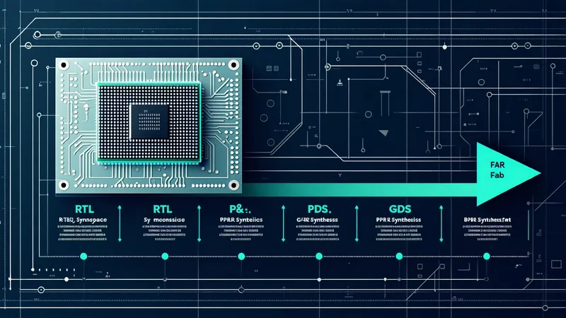
This guide covers the practical integration timeline for an OEM team bringing an OpenTitan-based root-of-trust block — as delivered by zeroRISC as a hardened, pre-validated IP core — into a new SoC design. The 8-10 week estimate in our headline assumes you have received a clean RTL delivery package from the IP provider and are integrating it into an existing SoC design that has already completed its top-level architecture. It does not cover the pre-tape-out security architecture design phase, which should complete before RTL delivery.
What the OpenTitan IP Block Actually Contains
The OpenTitan root-of-trust specification defines a set of hardware IP blocks that collectively implement the root-of-trust function. The primary blocks relevant to SoC integration are:
- ROM controller — manages the immutable boot ROM, implements integrity checking via a KMAC-based hash, and controls ROM execution permissions
- Key manager (keymgr) — implements the DICE-compliant CDI derivation ladder, managing hardware-backed key derivation from a root key through multiple boot stages
- OTP controller — manages one-time-programmable memory for lifecycle state, root key material, and device identity provisioning
- Lifecycle controller (lc_ctrl) — implements the silicon lifecycle state machine, handling transitions between RAW, TEST_UNLOCKED, DEV, PROD, PROD_END, and RMA states
- Alert handler — aggregates hardware alert signals from all IP blocks and escalates them through configurable escalation paths
- Cryptographic accelerators — AES, HMAC/SHA-2, KMAC/SHA-3, CSRNG (NIST SP 800-90A CTR_DRBG), ECDSA/P-384, RSA
- RISC-V Ibex core — the embedded 32-bit RISC-V processor that executes the ROM firmware and manages boot sequencing
These blocks communicate over a TileLink Uncached Lightweight (TL-UL) internal interconnect. The SoC integration surface is the peripheral bus bridge connecting TL-UL to your SoC's AHB-Lite or AXI4-Lite backbone, plus GPIO for alert escalation outputs and power/reset sequencing signals.
Week 1: RTL Delivery and Package Audit
The first week is largely administrative, but it sets the foundation for everything that follows. A complete RTL delivery package for an OpenTitan-based IP core should include:
- Verilog/SystemVerilog RTL source for all IP blocks, organized by block hierarchy
- Synthesis constraints (SDC format) for the process node(s) supported, with timing exceptions documented
- LEF/GDS abstract views for hardened cells (if any cells are hardened in the target process)
- DFT hook documentation: scan chain insertion points, BIST controller interface, ATPG test mode signal descriptions
- OTP memory map specification: which OTP word addresses correspond to which lifecycle state and provisioning fields
- Security policy document (for FIPS 140-3 validated deliveries)
- DV testbench package: UVM testbenches for the primary IP blocks, reference sequences, coverage plans
The first thing to verify is that the RTL package matches the version of the security policy document. A mismatch between RTL commit hash and security policy revision is a sign that either the IP was modified post-validation or the documentation is stale. Either condition requires clarification before proceeding.
Also verify that the synthesis constraints cover your foundry and process node specifically. Timing constraints written for TSMC 28nm HPM do not transfer directly to GF 22FDX without re-characterization; the library cell names, drive strength tables, and set_dont_touch annotations will differ. Most IP vendors provide foundry-specific constraint variants — confirm this before your synthesis team begins work.
Weeks 2-3: Bus Integration and Connectivity
The OpenTitan IP block interfaces to your SoC fabric through the TL-UL to AHB/AXI bridge. This bridge is a standard component, but its integration has several non-obvious requirements.
Address decoding. The OpenTitan IP has a defined address map for its internal registers. When this block is placed in your SoC memory map, the base address of the TL-UL bridge must be configured consistently with the address decode in your top-level crossbar. Mismatches here produce software-visible access faults that are straightforward to debug but time-consuming if discovered late.
Clock domain crossing. The OpenTitan IP typically operates on its own clock domain (the root-of-trust clock), which may be derived from a different source than your SoC main clock. The TL-UL bridge must include properly designed CDC (clock domain crossing) logic. The IP delivery package should document which interface signals cross clock domains and which synchronizer type is required. If your SoC integration team inserts additional CDC stages not in the original design, verify that the timing closure on the synchronizer paths does not introduce metastability exposure.
Reset sequencing. The OpenTitan lifecycle controller has a defined power-on reset sequence. The lc_ctrl block must be in reset before OTP initialization completes; premature release of the reset can result in an indeterminate lifecycle state read. Verify that your top-level reset tree sequences the RoT reset domain after the OTP macro's power-on settling time, using the timing values specified in the IP documentation.
Alert outputs. The alert handler outputs require connection to your SoC's system-level alert or interrupt fabric. The escalation outputs — which trigger actions like system-wide reset or CPU lockout on catastrophic security events — must be connected to functional logic. Leaving them unconnected or tied-off is a common integration error that eliminates the IP's tamper response functionality entirely.
Weeks 4-6: OTP Memory Map Configuration and DV Closure
The OTP controller is the most configuration-intensive component of the integration. The OTP macro itself is foundry-supplied; the OTP controller wraps it with access control, integrity verification, and the lifecycle/provisioning state machine. The memory map must be configured to match your SoC's provisioning requirements before DV closure.
Key configuration decisions include: the allocation of OTP partition space for root key material vs. lifecycle state vs. device-specific identity fields; the partition access policies (read-once, write-once, digest-locked); and the test vector set for OTP programming verification. The IP delivery package includes a reference OTP memory map specification, but OEMs typically need to customize it based on their provisioning flow and the specific identity fields their system requires.
DV (design verification) for an OpenTitan-based integration runs at two levels. The block-level UVM testbenches in the delivery package cover the individual IP blocks against their block-level specifications. The integration-level verification — covering the assembled SoC context, including clock/reset sequencing, bus transactions, and alert propagation — is the OEM's responsibility. The delivery package provides reference sequences that can seed the integration-level testbench, but coverage closure on the integration context requires OEM-specific test development.
A practical scenario: an SoC team at a mid-size IoT semiconductor company targeting TSMC 28nm HPM ran their integration DV from week 4 through week 7, ultimately requiring a respin of their reset sequencing logic after the OTP initialization timing margin proved insufficient under worst-case slow corner analysis. The root cause was that the initial integration used the OTP settling time from the IP documentation's typical-case value rather than the slow-corner worst case. This is a common finding; the timing margin analysis for OTP power-on settling must use PVT corner-specific values, not typical-case values from the IP datasheet.
FPGA Prototyping: When It Helps and When It Misleads
Many SoC teams include an FPGA prototyping phase before silicon tapeout to enable firmware development to proceed in parallel with silicon DV closure. OpenTitan-based IP blocks can be mapped to Xilinx UltraScale+ or Intel Agilex FPGA targets with some modifications. The critical caveat is that FPGA prototyping does not validate physical security properties.
The OTP macro on an FPGA prototype is typically implemented as a block RAM with write-once behavior enforced in firmware — not as an actual one-time-programmable fuse array. This means that lifecycle state transitions on the FPGA prototype do not exercise the actual OTP programming path or the read-after-program verification. Similarly, the entropy source on an FPGA prototype is typically based on a ring oscillator TRNG that has different statistical properties than the SP 800-90B-qualified noise source in the RTL delivery. Firmware developed on the FPGA prototype should not assume that random number generation timing or OTP access timing will match silicon.
We are not suggesting that FPGA prototyping is not valuable — it is, particularly for firmware development and system-level functional testing. But FPGA prototype results should not be used to close DV on security-critical paths, and OTP-related behavior on the FPGA prototype should be clearly flagged in firmware as non-representative of silicon behavior.
Weeks 7-10: Silicon Bring-Up and Tapeout Checklist
The final phase before GDS submission covers synthesis closure, DRC/LVS signoff, and the root-of-trust specific tapeout checklist items. The synthesis closure step for the RoT block deserves attention: the cryptographic accelerators contain datapath structures — particularly in AES S-box implementations and SHA-3 permutation logic — that synthesis tools may retime aggressively in ways that could affect side-channel properties if the constraints do not include explicit set_dont_touch or set_max_delay annotations on sensitive paths. Review the synthesis constraints documentation carefully for these annotations.
For the tapeout checklist, the root-of-trust specific items include: verification that the cryptographic boundary is correctly defined in the GDS versus the security policy documentation; that the tamper mesh (if implemented as a hard macro or metal layer) is correctly connected; that the OTP macro's anti-fuse isolation from the analog domain is correctly implemented per the foundry PDK guidelines; and that the JTAG debug access port is configured in its locked state for production (PROD) lifecycle state.
First silicon bring-up for an OpenTitan-based design should include a dedicated RoT bringup script sequence that exercises lifecycle state readback, OTP partition integrity checks, and a basic DRBG health test — all before any application firmware is loaded. These checks confirm that the silicon lifecycle state is correct (typically PROD for production units, DEV for engineering samples) and that the entropy source is operational. Catching a non-functional entropy source at first silicon is far preferable to discovering it during firmware bring-up or, worse, in field units.
The Questions That Get Asked Late
After working through several integration engagements, certain questions surface consistently in the final weeks before tapeout that should have been resolved during architecture phase:
Can we add custom commands to the lifecycle controller? No, not without affecting the validation status. The lifecycle controller state machine is a fixed specification; modifications to it take the implementation outside the scope of the FIPS 140-3 validation. If your OEM application requires custom lifecycle behavior, that logic must be external to the certified IP block.
Can we disable specific cryptographic accelerators to save area? Disabling accelerators affects the module's approved algorithm list. If your application requires only a subset of the accelerators (e.g., only AES and HMAC, not ECDSA), this must be addressed in the integration configuration before the security policy is finalized — not as a post-facto netlist modification.
What happens to the FIPS validation if we change foundry? A foundry change constitutes an environmental change relative to the validation documentation. The IP provider should have documentation on which parameter changes require re-evaluation and which are covered by the existing security policy's environmental assumptions. Typically, a change from one supported foundry to another supported foundry (both listed in the security policy) does not require a new CMVP validation; a change to an unsupported foundry requires at minimum a security policy amendment.
The integration timeline is achievable — 8-10 weeks from RTL delivery to tapeout-ready integration is realistic for a well-prepared team. The teams that miss that window most often do so not because of technical complexity in the IP itself, but because of late resolution of the configuration and interface questions above. Resolving those in week one, not week eight, is what makes the timeline hold.